![]()
|
|
|
|
Welcome to Spiceguy.net.
Signal Integrity This page shows how to set up noise simulations using SSTL buffer as example. 1) Background on Noise and Ground Bounce
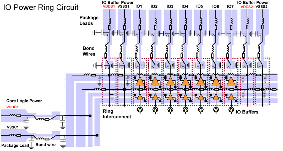
Noise and ground bounce failures are mainly cause by multiple simultaneously switching outputs (SSO). Since Input/Output (I/O) buffers are larger than core logic standard cells, they are usually placed around the perimeter of the chip. Noise occurs from the large switching currents passing through the pad bond wire and package lead inductances. Accurate SPICE simulation of the IO ring for SSO and ground bounce requires insertion of the IO ring RLC parasitics (as well as mutual inductance "M"), all the I/O buffers, and the package model. Noise occurs when many output buffers switch together causing large voltage spikes. If there are insufficient power and ground pins, unstable voltage can occur at the I/O buffers. Another problem cause by package parasitics is inductive crosstalk induced delay between the I/O signals having closely spaced package traces. To set up SSO SPICE simulations one needs to make RLC models of the package and power ring traces. Unfortunately most parasitic extraction tools do not extract inductance (L), and these inductances need to be modeled by hand if they cannot be extracted. The following schematic takes all these considerations into account. Across the top we have a set of VDD/VSS pads on the left, followed by seven I/O pads, and another set of VDD/VSS pads on the right. The VDD/VSS supplies on the top are wired to the outermost power rings, which deliver power only to the I/O buffers. The VDD/VSS supplies on the left side are connected to the innermost power rings, which supply power to core logic and standard cells. This structure is what needs to be simulated
(IO Power Ring. Click image to enlarge.)
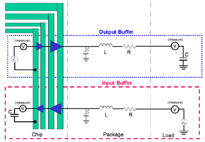
The next step is to add drivers (voltage sources) to the simulation to switch the desired buffers. For example, one setup may have six of the seven outputs switching together while the 7th output is biased to remain low (at Logic-0). During switching we can monitor the effect of the six SSO outputs on the quiet output as shown in the next section's SSTL noise simulation. That particular setup had up to 870mV spikes on the quiet output which was biased at Logic-0. In addition to monitoring the quiet output, voltage and current levels should be measured at the input and output of each I/O buffer as shown in the next schematic to help understand the cause of noise and ground bounce. By iterating these simulations, an optimal hookup can be determined with minimal noise. This result can determine:
(IO Buffer voltage and measurement points. Click image to enlarge.)
2) SSTL Buffer Noise Simulations
These plots are for SSTL Bidirectional buffers used in a ASIC to Memory interface to simulate the effects of noise on the output's duty cycle. Voltage and current waveforms are shown for five buffers switching simultaneously (SSO). Hookup is for Class-1 and Class-2 buffers driving 43Ω series resistor; 3" transmission line; and 10 pF termination load.
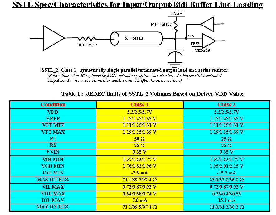
A) SSTL SPEC FOR CLASS 1 AND CLASS 2 SSTL
This table shows the SSTL spec for voltages, current and resistance for Class 1 and Class 2 SSTL buffers. Schematic shows hookup with loading & termination.
(SSTL SPEC. Click image to enlarge)
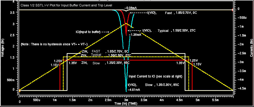
B) SSTL IV PLOT FOR INPUT DC TRIP LEVELS This plot shows I-V curve (best/typical/worst case) for Class 1 and 2 bidirectional SSTL buffer when tri-stated, and port “IO” is used as input buffer with “ZI” as the buffered signal. Input voltage trip levels are also shown, and are measured to be the same as VREF = VDD/2. These trip levels fall between VIL(max)=0.93V and VIH(min)=1.57V listed in Table 1, Page 4, and play an important role in ground bounce noise immunity where the input noise trips the input stage and results in oscillations fed back to output stage. (SSTL DC TRIP POINTS: Click image to enlarge)
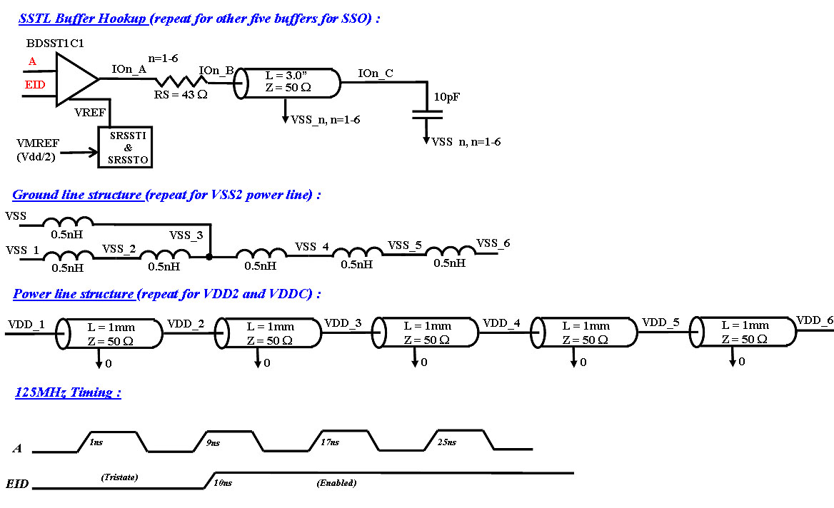
C) SPICE Hookup & Timing for 125 MHz Noise Simulation
(SSTL HOOKUP: Click image to enlarge)
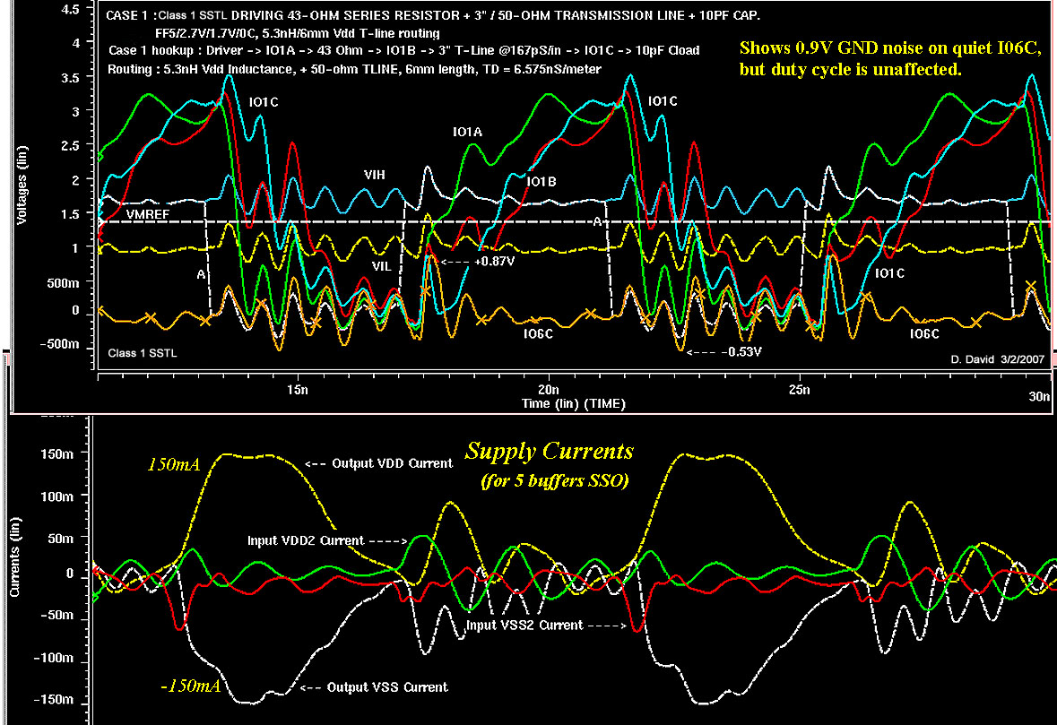
D) Class-1 SSTL Noise Plot, Best Case, 2.7/1.7V, LVDD = 5.3nH, 5-SSO and 1-low
The following plot shows a Class 1 SSTL Buffer driving the loading shown in above schematic with 3" transmission line and 5.3nH inductance. Five outputs (IO1-IO5) are switching, while the sixth output (IO6) remains low.
(SSTL NOISE SIMULATION: Click image to enlarge)
|
|
Send email to Doran@Spiceguy.net with questions or comments about this web site. Copyright © 2011 by Spiceguy.net. Last modified: 4/10/11 |