![]()
|
|
|
|
Welcome to Spiceguy.net.
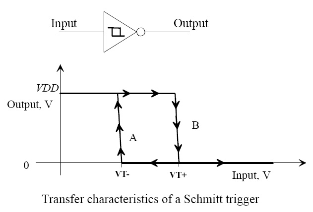
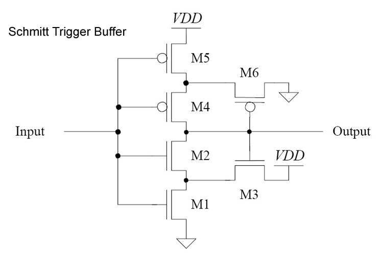
Hysteresis Simulation This page illustrates how to Simulate a Schmitt Buffer using HSPICE and Plot the Hysteresis Loop using (slow) Transient or DC Analysis.
The above measure statements will generate the hysteresis levels numerically. To see these results graphically with the familiar hysteresis loop, see these images below for illustration:
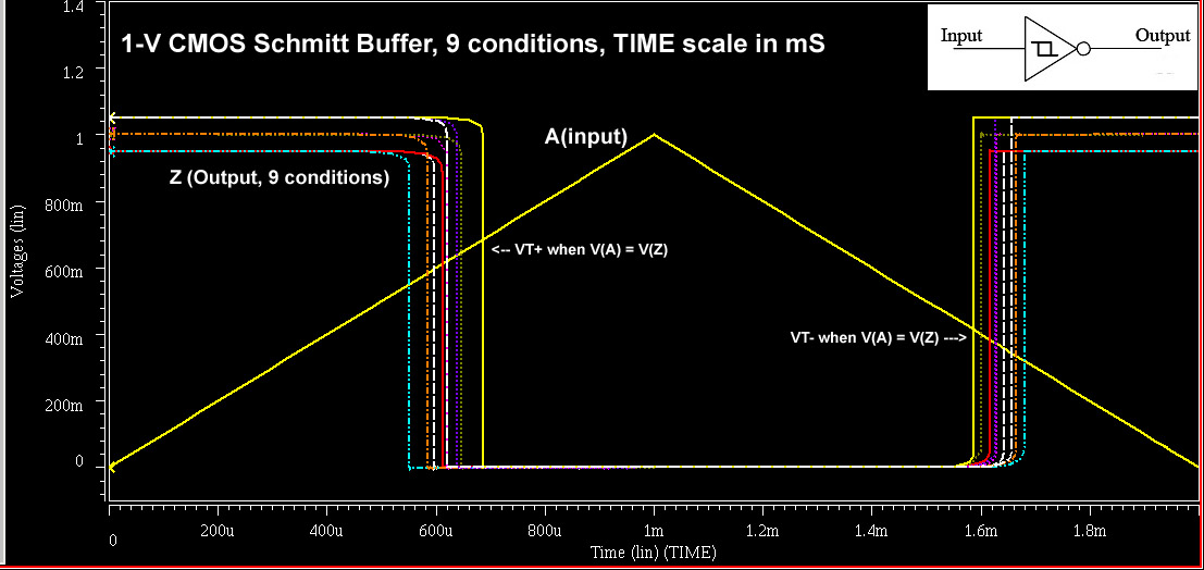
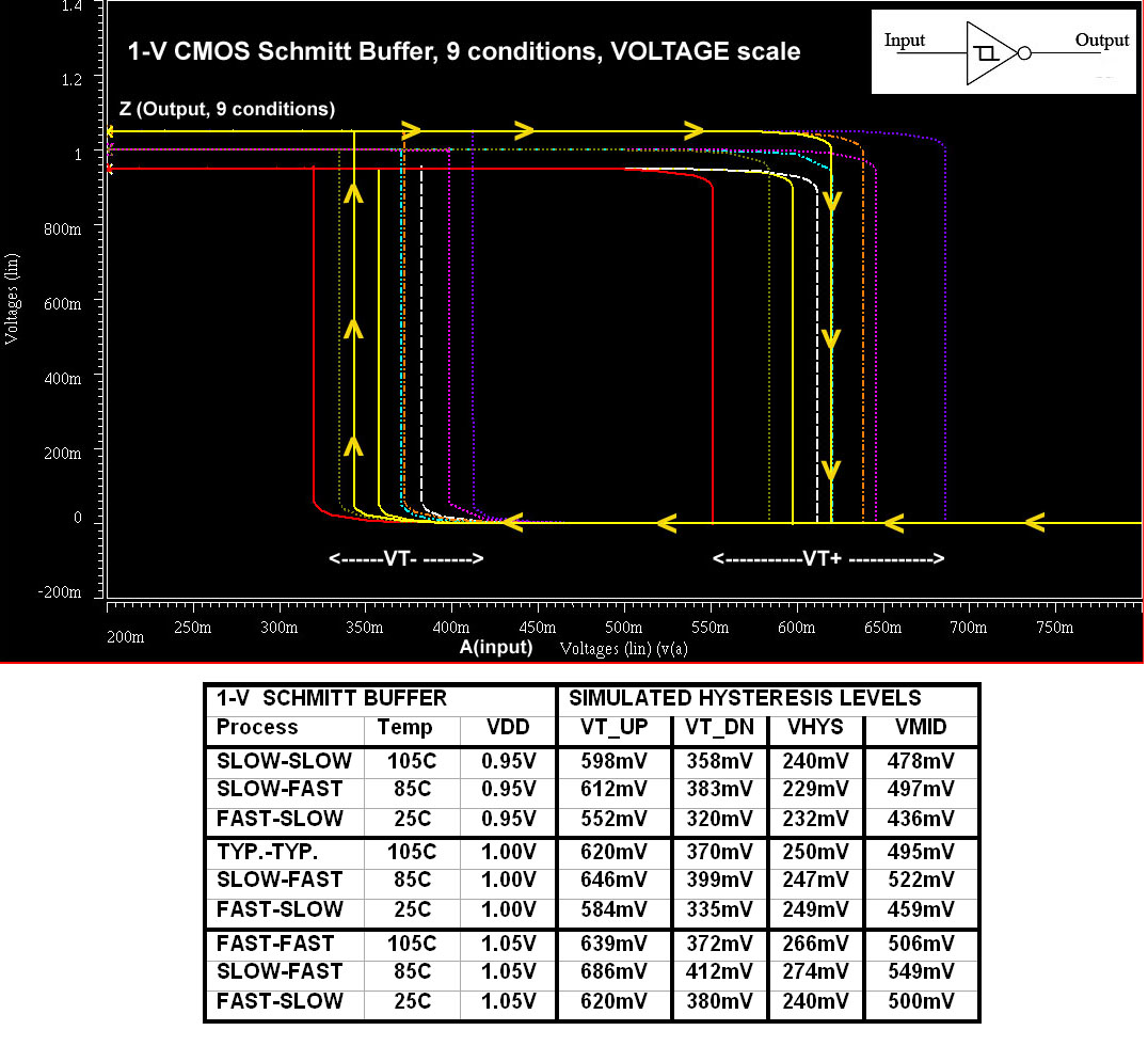
A) This image shows our transient simulation with TIME on the X-Axis. We don't get the familiar hysteresis loop, but it's exactly what we simulated with the triangle input. You can graphically measure the trip points where the input crosses the output, or V(A) = V(Z).
(TRAN. ANALYSIS: Click image to enlarge)
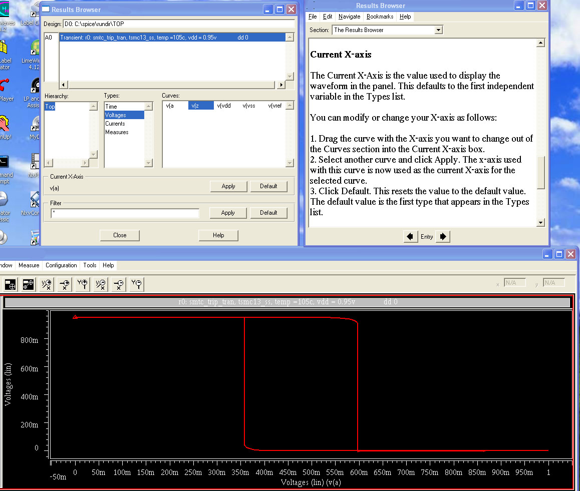
B) This image has instructions you need in AvanWaves to change your X-Axis from "Time" to Voltage V(A) using alternate DC analysis. Repeat this process for all runs and plot V(A) on the X-Axis, and then select V(Z) for each run.
(DC ANALYSIS: Click image to enlarge)
C) Above procedure can be repeated to generate desired plot with hysteresis loops for all runs. Below this plot follows a table of measured hysteresis levels (from HSPICE output) for my nine chosen process/voltage/temperature (PVT) conditions. Note: Skewed process models were used for worst case trip variations with P-Channel stated first, Ex: SLOW-SLOW means slow PCH/slow NCH.
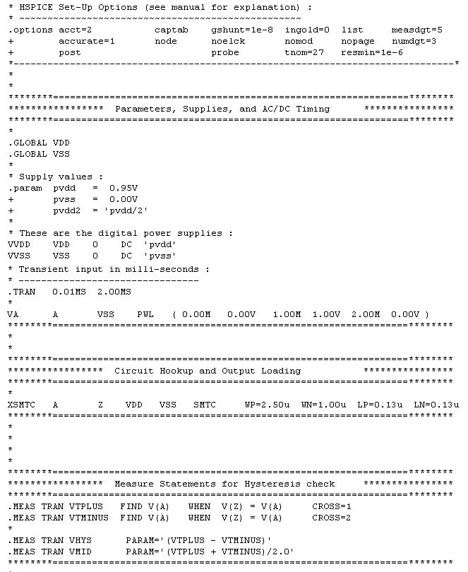
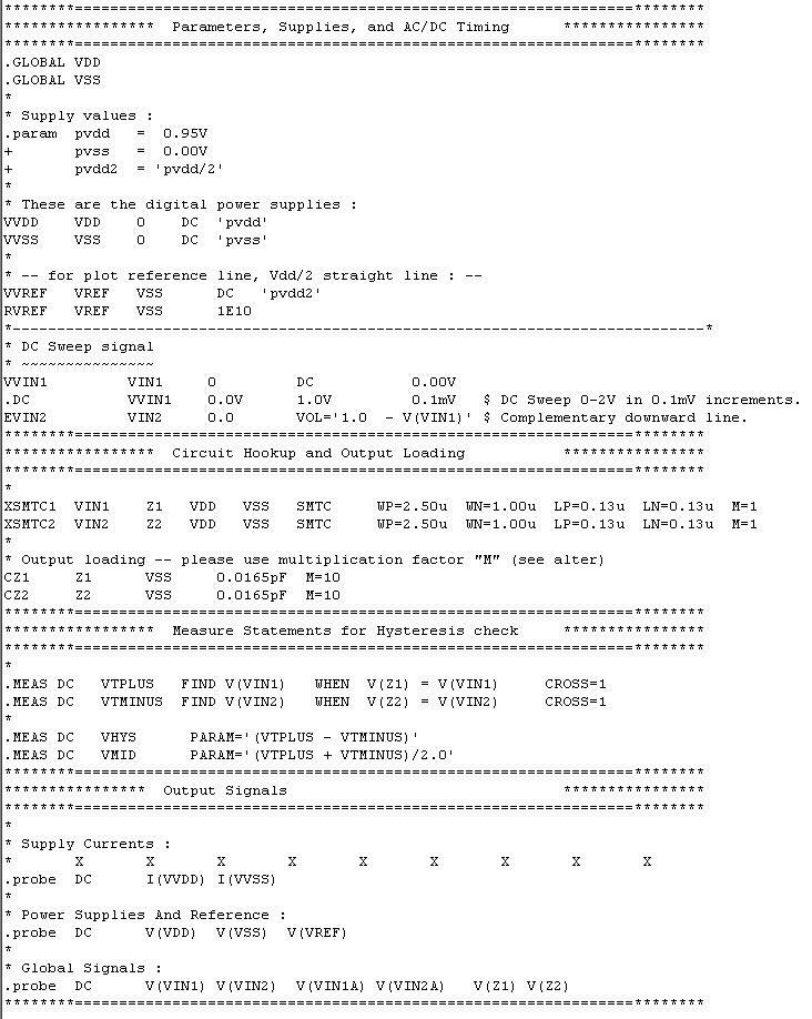
D) Shown below is a portion of the HSPICE source deck used to generate these plots. First one is transient, and the second is DC analysis.
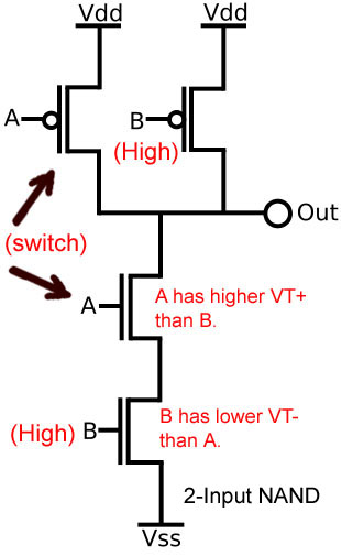
Note : Above simulation is also good for checking trip levels of gates without hysteresis. Thus, you can use this setup to see if there is any hysteresis on a gate. If not, then you get equal positive (VT+) and negative (VT-) trip points (i.e., with VHYS = 0). For gates with more than one input, remember to repeat the trip measurement for each input individually since trip points will vary depending how far that input device is from the output. See below for Nand gate structure.
Nand Gate Structure
|
|
Send email to Doran@Spiceguy.net with questions or comments about this web site. Copyright © 2011 by Spiceguy.net. Last modified: 12/09/11 |